


Old Price Road cuts a stark divide through the Arizona desert on its nearly straight north-south run. West, green fields give way to beige sand. Beyond, the Sierra Estrella mountains dominate the nearly flat landscape. On the other side of the road, a network of pipes connects a series of massive buildings, giving everything a vaguely steampunk vibe. This is Intel’s Ocotillo site in Chandler, Arizona, home of some of the company’s chip fabrication facilities — called fabs — including one where the company makes its new Panther Lake chips.
As part of my time at Intel’s 2025 Tech Tour in Arizona earlier this month, I got to tour the Ocotillo site and venture into the new Fab 52 for an inside look at chip fabrication. The tour began with a loop around the company’s Arizona campus, which is just over one square mile in size and contains multiple fabrication sites. All of the campus roads sport chip-related names like Silicon Street, Processor Parkway, and Transistor Terrace.
A view of the Sierra Estrella from Intel’s Ocotillo campus.
The campus also features tons of covered parking — a blessing in the summer when temperatures soar as high as 45°C. But more than just covering the cars, it’s also solar panels. The energy Intel captures this way is given back to the city of Chandler.
This isn’t Intel’s only sustainability effort in Arizona. Another part of the campus we saw was the on-site water treatment and recycling facilities, as well as the Ocotillo Brine Reduction Facility (OBRF). The OBRF removes salt from the water before further treatment, and the removed salt can be reused — Intel sells it to other companies.
A view of the water treatment and piping on Intel’s Ocotillo campus.
The 12-acre treatment facility, a partnership between Intel Chandler, treats nine million gallons of water per day and returns it to the factory as a very clean water source. Water is distributed around the Ocotillo site via a water distribution loop — some of the aforementioned piping around the buildings. Fabs use millions of gallons of water daily for a variety of tasks, including cleaning the silicon wafers used to make chips, for cooling, and more.
Moreover, Intel is water positive in Arizona, conserving water within its operations while also funding community-based water restoration projects. In 2023, these projects restored 1.1 billion gallons (4.16 billion litres) of water to the state.
Power generation on the Ocotillo campus.
The Ocotillo campus also has its own power plant, supplying roughly 100 megawatts of electricity for the site.
Gowning up to head inside
With the external tour wrapped, we headed inside to see Fab 52. The sheer scale of the facility was overwhelming, especially considering how small the final product is. Our guide noted that it’s over a mile (1.6km) across the whole fab, and the entire facility is walkable.
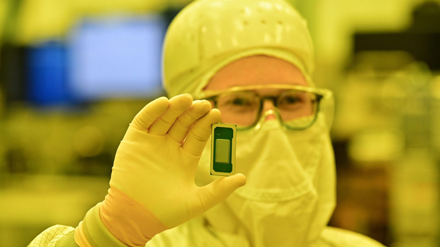
But before we got inside, we had to gear up. Fab 52, like many fabs, must be kept incredibly clean as even the smallest particles of dust can be catastrophic for the delicate circuitry on computer chips.
Intel workers wearing gowns inside the fab’s cleanroom environment. | Image credit: Intel.
Fab 52 is a class 10 clean room, which means it’s about 100 times cleaner than an operating room, with air circulated six times per minute. More than that, the entire facility is designed for specific air movement, with clean air piped in through the ceiling and the floor composed of perforated metal tiles that allow the air to vent out.
But dust and dirt aren’t the only concerns. We couldn’t bring in any wireless devices like phones or even smartwatches due to potential interference. Even copper was restricted, with some workers in the fab wearing pink suits to designate them as able to work with copper to avoid contaminating non-copper areas. Intel also wouldn’t allow us to bring in cameras, mostly due to IP protection since Intel also makes chips for other companies in the fab — while disappointing, the company did provide ample photos of the inside of Fab 52, which you’ll see throughout this story.
A worker completes tasks on a computer inside Intel’s Fab 52. | Image credit: Intel.
With all of our tech securely stored, we headed up to the fab entrance. Getting into the fab meant going through a series of doors that felt almost like an airlock on a spaceship. Inside the doors was a gowning area where we all had to dress before entering the fab itself. Every person who enters must wear hair and/or beard nets, a body suit, a hood, two pairs of boots, two pairs of gloves, and safety glasses.
Once gowned, all that remained exposed was a narrow strip of our face, including our eyes and nose. The suits themselves weren’t cumbersome and actually were really light, but with everything on, they got quite warm. While we only wore the suits for at most 30 minutes, those who work in the fabs wear them for hours at a time and have to de- and re-gown every time they leave the fab, such as to use the washroom or to eat lunch. It took us a while to get through the gowning process, but for those working in the fab, it’s almost second nature, and they can gown up in under five minutes.
Automated systems carry silicon around the fab
Equipment inside Fab 52. | Image credit: Intel.
Inside the fab was like stepping into a totally different world, an advanced future techscape. The lighting was weirdly yellow — for a good reason! — and everywhere I looked, machines whirred, lights blinked, and people suited up like me bustled. Overhead, vehicles slightly larger than your average carry-on suitcase zipped along on a monorail system.
The overhead monorail is part of an automated material handling system (AMHS) that utilizes overhead hoist transports (OHTs) with front-opening unified pods (FOUPs) to carry materials, such as silicon wafers, around the fab. It was mesmerizing watching the AMHS in action as the OHTs zipped along the rail. At intersections, the OHTs looked about to collide, but at the last second, one would slow slightly, allowing the other to pass safely, before rapidly picking up speed again.
Image credit: Intel.
Intel’s Fab 52 has over 30 miles (48.3 km) of AMHS to deliver wafers directly to parts of the fab, like the extreme ultraviolet (EUV) lithography machines. These machines are used to etch patterns on the silicon, which form the inner workings of computer chips. The video below offers a decent basic explanation of the chipmaking process and even shows what the OHT and FOUPs look like.
These massive EUV machines can measure roughly 33 x 17 x 13 feet, weigh more than 330,000 pounds, and cost between US$150 and US$380 million (about C$210 to C$533 million). Intel said it takes 14 weeks from the arrival of these tools until they’re able to start production in the fab, and the company uses special sealed elevators to clean the components and transition them into the cleanroom. The EUV machines are installed in sections with specialized rigid construction to minimize vibrations, which can also negatively impact the etching process.
One of the EUV lithography machines inside Fab 52. | Image credit: Intel.
As mentioned earlier, the fab’s odd yellow lighting is actually an important addition that both aids the lithography process and boosts human vision. First, lithography relies on a photosensitive material dubbed photoresist that reacts to certain wavelengths of light. The yellow light used in fabs have wavelengths beyond the sensitivity of the photoresist, which means exposure to the lighting won’t impact the lithography process.
Moreover, human eyes have better visibility in this type of lighting — red lighting can make it harder to recognize details, while green light can cause glare. The yellow lighting strikes a balance for better visibility without interfering with lithography and photoresist materials.
Intel’s history in Arizona
An outside look at Fab 52.
Intel first started operations in Arizona back in 1979 and has since invested US$50 billion (roughly C$70 billion) in its operations there, helping establish the region as a major semiconductor manufacturing hub.
Intel’s Arizona campus is just over one square mile in size and contains multiple fabrication sites, including:
Fab 12, opened in the 1990s and became one of Intel’s most advanced manufacturing facilities.
Fab 22, opened in 1996.
Fab 32, constructed in the early 2000s.
Fab 42, completed in 2017.
Fab 52, which broke ground in 2021 and is now in operation.
Fab 62, part of the expansion that included Fab 52.
It takes three to five years to build a typical fab at a cost of US$20 to $25 billion (about C$28 to $35 billion). It’s not hard to see why, with all the equipment and specialized tooling required to make chips. And again, it’s hard to overstate the scale of the infrastructure used to create these minuscule chips that power the devices we use every day.
Intel chips power laptops, desktops, and tons of other electronics — and that’s just Intel! There are several other chipmakers out there creating silicon for millions of devices from smartphones to earbuds and more. It’s a little bit insane how much goes into creating something most people use daily without thinking about it.
MobileSyrup may earn a commission from purchases made via our links, which helps fund the journalism we provide free on our website. These links do not influence our editorial content. Support us here.
