


Intro
In July 2025, we from Neodyme got together in Munich and did security research on a bunch of IoT devices, ranging from bluetooth headsets, to door locks, to drones. One of these was the Potensic Atom 2. It’s a photo and video drone with a gimbal-stabilized 4K camera and a remote control that you hook up to your own smartphone and the proprietary app. If you’ve ever flown a DJI Mini 4K, this drone will look very familiar to you.
Potensic Atom 2
This post is part of a two-part series that will cover how we disassembled the drone and dumped the firmware from the NAND chip and how we analyzed the drone’s firmware, app, and remote control to find some backdoors and vulnerabilities.
Goal: Dumping the Firmware
One of the most important pieces of information you can acquire when setting up to hack a device is its firmware. If you want to reverse engineer the software that’s running on the drone and find vulnerabilities in that, then you need a copy of it in the first place.
Now there are a couple of ways to go about that, some are less intrusive and some are more effective.
You might get lucky and be able to just download the firmware as a firmware update from the manufacturer’s website. However, those update sites are often not publicly documented and can be locked behind authorization checks or encrypted. Encrypted firmwares can still be useful – you “just” need to reverse engineer the on-device decryption process. For the Atom 2, downloading the firmware updates required having a valid drone and remote control serial number and the firmware update was also encrypted. Without having the decryption logic, we put this approach on ice during our initial research.
Another really comfortable approach is to use exposed debug interfaces like JTAG or UART. However, those are often undocumented, unlabeled, or entirely removed for public versions. We didn’t find any on the Atom 2.
What we can always do, though not necessarily always successful, is solder off the entire NAND chip and dump the firmware byte by byte. This has the risk of breaking the NAND chip and/or the rest of the board if you’re not careful. Also, some devices, like modern smart phones, encrypt their persistent storage with key material stored in, e.g., the TPM. If that is the case, then simply soldering off the NAND chip will leave you with unusable encrypted data. Fortunately, the Atom 2’s NAND contents are not encrypted, as we find out later.
Dumping the NAND Chip
Dumping a NAND chip generally always follows the same pattern:
Identifying the NAND Chip
Removing it from the board
Identifying the data pins and communication protocol of the NAND chip
Connecting the NAND chip to some kind of reading device
Reading the NAND content
Reassembling the read contents into a working firmware – usually containing one or more file systems
Identifying the NAND Chip
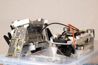
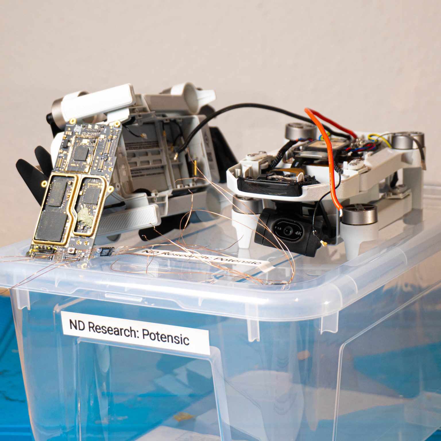
The Atom 2 has multiple boards:
Top side of the drone
Bottom side of the drone, with the mainboard and some of its RF shields already removed
We are mainly interested in the main board because that’s where the NAND flash is going to be. The main board had several metal RF shields that we have already pried off or cut through on the photos.
We can identify most of these chips through their markings. Note that while we’re mainly interested in the NAND chip, knowing the others can help with recognizing things during reversing later on. Roughly knowing which SoC we were working with was crucial, as you will see in later sections of this blog post.
(Note that the markings below might not match the photos completely. We had multiple drones. The markings are mostly from the first drone and the photos are mostly of the second drone.)
Top-side
Top side of the mainboard, with all RF shields removed
SoC (System on a Chip, aka “the main thingy”)
Markings: 23AP10 VTQMSQKJYJ 4978-CN B3
We didn’t find an exact match, but this site references the 21AP10.
The page title is 21AP10 SS928 平替SD3403V100 海思 SOC芯片
21AP10 SS928 平替 => 21AP10 SS928 Drop-In Replacement
SD3403V100 海思 SOC芯片 => HiSilicon SD3403V100 SOC Chip
That is a mobile camera SoC.
It makes sense that this is the SoC because it is close to both external RAM chips and the NAND flash.
In this teardown of a previous Atom model, the device had a HiSilicon Hi 3559 camera MCU
We found a data sheet for the HiSilicon Hi3519 V100.
Close enough for now.
RAM
Markings: SEC340 K4A8G16 5WC BCTD G2F9190AC
Data sheet can be found on the internet.
ARM Cortex-M4
Markings: GD32F470 VGH6 BUMK618 AL2451 GigaDevice ARM
Data sheet can be found on the internet.
Might be SD-card related since the SD card slot is on the other side.
Unknown Chips
Markings: V2 2441TM4N190.00
The name 2441TM appears in some WizSense surveillance cameras
Not sure if related
2 chips with markings: 8285HE 426656 CS2441
Bottom Side
Bottom side of the mainboard, with all RF shields removed
NAND flash
Markings: MXIC X243662 MX35UF4GE4AD-241 5P231800A1
Data sheet can be found on the internet.
RAM
Markings: SEC407 K4A8G16 5WC BCTD G2K43304C
Same as on top side
ARM Cortex-M4
Markings: F460JEUA P8VR4400 2416021
Not sure what it’s used for.
A data sheet for the HC32F460JEUA-QFN48TR (looks close enough?) can be found on the internet.
WLAN + Bluetooth
RTL8821CS
Data sheet can be found on the internet.
Removing the NAND Chip from the board
Now that we have identified the NAND chip, we fasten the board and tape off the remaining components with heat-shielding tape.
Drone and mainboard, partially taped off with heat-shielding tape. The mainboard was still connected via the flex cable while we were searching for debug pins.
Usually getting the chip off of the board is just a matter of using hot air station and flux. However, you can see on the photos that the chip is actually glued to the main board with what is probably epoxy. That’s a thing you can do if you want to secure the chips more securely and not depend on the solder joints to hold your chip in place (and risk breaking them). Or you can do that just to the NAND chip to make it harder for researcher to pry off your NAND chip and dump your firmware.
Anyway, a few cuts with a sharp knife, some heat and a generous amount of flux later, the little bugger came off in one piece.
(And with it, a couple of extremely tiny resistors that I knocked off with my pliers and promptly lost. This main board is now broken. But don’t worry, through the magic of buying two three of them, we can still fly the drone.)
As you can see, this chip has a large ground pad in the middle. This allows the chip to transfer a lot of heat to the ground plane in the mainboard, which makes soldering it off a little harder.
Identifying the data pins and communication protocol of the NAND chip
According to the data sheet of the MX35UF4GE4AD NAND chip, the flash chip can either come in a 24-pin BGA package or an 8-pin WSON package, which we have here. A quick look at the pin descriptions tell us that the NAND chip is communicating via SPI.
Pin SymbolPin DescriptionCS#Chip SelectSISerial Data InputSOSerial Data OutputSCLKClock InputWP#Write protectionHOLD#HoldVCCPower Supply (1.8 V)GNDGroundDNUDo Not Use
Well, let’s solder tiny copper cables to all of those pins and drown them in a bit of hot glue to stop them from breaking off.
Note that you can get a proper socket for 8-WSON chips into which you simply clamp the chip and which exposes easy-to-work-with breakout pins. None of our sockets we brought fit though, so we just did it the old-school way.
Connecting the NAND chip to some kind of reading device
SPI is pretty easy to work with. We have two main data lines called SI and SO (Serial In/Out). You will also find them under the names “MOSI” and “MISO” (Master Out Slave In / Master In Slave Out). As the names of these suggest, SPI follows a master-slave architecture. The microcontroller drives the communication and the peripheral device reacts.
Fortunately, we are simulating the microcontroller-side of the communication, which means that we have a large amount of control. Specifically, we control the clock (SCLK). Sometimes it is hard to talk to embedded hardware because of the speed at which they operate. With SPI, however, we can slow down the clock to however fast we want the devices to talk.
Since SPI is a bus protocol, more than one slave device can be hooked up to a master device on the same data lines. To avoid collisions, each device is also assigned its own “Chip Select” line (CS). When the master device wants to talk to a specific slave device, it pulls the corresponding CS line low. Devices that have their CS line high won’t react at all.
Obviously there are fancy devices on the market that will make dumping a NAND chip via SPI pretty easy and straightforward. Problem is, we couldn’t get any of them to work. They either didn’t fit (physically), were too fast or failed for some other strange reason we didn’t understand. So we wrote our own dump script onto an ESP32 using the SPI commands in the data sheet and let it forward the data to our computer via the USB console.
Doing that, we ended up with a 544 MiB dump, containing 131,072 pages of 4096+256 bytes. (We will come back to that “+256” later on.)
Let’s dig into what this the flash dump contains with binwalk:
Binwalk output of the raw NAND dump
Sweet! We get a working ASCII copyright string, so something must have worked. And at the end of the image we have a bunch of UBIFS images. That’s probably where all the juicy files are!
Let’s extract them with dd and take a look inside with ubi_reader:
Extracting the the first UBI image from the NAND flash dump via dd. Note that the offsets don’t match the binwalk output directly because we are using a bigger blocksize to speed this up (bs=1024).
ubi_reader finds three file systems but fails to extract any files from them before crashing
Hmm. That doesn’t work. Spoiler: The extracted image is broken.
Now if you’ve ever done something as hacky as this, you will know about a pesky little phenomenon that happens when you just solder copper wires onto a chip, stick that onto the ports of an ESP32 and do SPI communication – which has no built-in integrity checks.
Random Bit Flips
These are three dumps taken from the same NAND chip:
The MD5 hashes of the three separate dumps from the same NAND chip are different, indicating that our reading process introduces bit errors.
If you read 4 MiB of data from the chip, not all of the bits you receive are correct. And without any additional data, you have little way of knowing which ones are correct and which are not. If you are lucky, then the dumped data will still “work”, i.e., the contained file system will mount and you can browse files, but futher down the line you will have no way of knowing whether that weird function you’re reversing is actually weird or just the product of random bit flips messing up the CPU instructions.
A relatively simple yet time-consuming way to get around this: Read the flash often (at least three times) and hold a majority vote for every bit. Since the bit flips are random and not too prevalent, they are less likely to hit the same bit twice.
Hot tip: If you’re gonna work with python, use numpy and work on arrays and memory-mapped files. Otherwise this can take a lot of time and a lot of RAM – even for a 512 MiB flash dump.
import numpy as np
import sys
if len(sys.argv) != 4:
print(f”Usage: {sys.argv[0]} dump1 dump2 dump3″, file=sys.stderr)
sys.exit(1)
dump_filenames = sys.argv[1:]
a, b, c = [np.memmap(f, dtype=np.uint8, mode=”r”) for f in dump_filenames]
majority = np.memmap(
“dump-majority-voting.bin”,
dtype=np.uint8,
mode=”write”,
shape=(a.size,),
)
# quick three-way majority voting
majority[:] = np.where(
(a == b) | (a == c) | (b != c),
a,
b,
)
After majority-voting, we get a different MD5 sum. This one remains stable even when pulling more samples.
But isn’t there a better way? Yes, there is. And – btw – even with completely correct majority voting, the flash content is still broken. But we’ll get to that.
Trying to work with the majority-voted dump:
Binwalk output on the majority-voted NAND dump
Trying to parse the UBI image with ubi_reader still fails – this time even before finding any file systems (wtf?)
Out-of-band bytes and ECC troubles
One thing we have have silently brushed aside for now: The NAND chip distinguishes between “user data” and “extra data”. In our dump above, we have naively concatenated it all together and assumed that a page size of 4096+256 bytes somehow makes sense. Of course, it doesn’t.
Also, this majority voting hack is obviously not the “correct” way to work with a NAND chip. And even the proper SoC mounted on the proper mainboard can’t run a system off of a flash chip that gives it random bit flips that it can’t detect or recover from. The problem is that NAND is just inherently imperfect storage. Majority voting only corrects for transmission errors during dumping, but does nothing to bit errors that are stored on the device! Bits on the storage might decay over time, or the CPU might also have some transmission errors during writing.
Of course this problem has been very well known for a long time, so manufacturers always include some extra space next to user data for “error correction”. These extra bytes are called “out-of-band” bytes. And they are used to implement Error Correction Codes (ECC).
ECC according to the NAND chip data sheet
The flash chip implements its own error correction algorithm by reserving some of the space for ECC. It is split into
2048 blocks of
64 pages of
4096 user data bytes + 256 “extra” bytes (aka out-of-band bytes)
=> 512 MiB of user data (the chip is 4 Gb, not 4 GB)
=> 32 MiB of extra data
If the chip-internal ECC is enabled, some of those extra bytes are used for ECC.
At this point, we naively assumed that each page would be
4096 bytes of user data followed by
256 (or less?) bytes of ECC covering the previous 4096 bytes.
However, we quickly found out that the sequences classified as “extra data” contain readable strings! That definitely suggests that this isn’t ECC data.
In-page addresses at and above 0x1000 (= 4096) are extra data
You can also see that there are parts within the user data where strings are suddenly cut off. This suggests that the ECC layout we assumed was wrong. It took us quite a while to figure out what exactly we missed.
Text “ignoring the CPU number” cut off at 0x824
Text “IRQ_WAKE_THREAD” cut off at 0x824
Entropy Analysis
Turns out, the ECC layout is not just 4096 bytes of user data followed by 256 bytes of ECC. If we put all pages next to each other and then calculate the entropy over each n-th byte of a page, we will find that there are multiple sections with high entropy:
Why are we looking at entropy? Well, because we expect the user data to have ASCII text (low entropy) every now and then and the ECC data to be mostly random-looking byte values (high entropy).
The graph we’re seeing up here suggests that there are sections of roughly 1 KiB of user data, followed by 28 bytes of ECC data. Specifically,
1028 B user data + 28 B ECC
1028 B user data + 28 B ECC
1028 B user data + 28 B ECC
1014 B user data + 28 B ECC
142 B unused
Why these stranges values? And which ECC algorithm is that? We can choose to ignore that and just extract the user data sections and stitch them together. I won’t spam you with more binwalk and dd screenshots and just tell you that that also won’t result in a readable UBIFS image. Fortunately, we find an explanation for these values in the next section!
ECC according to the SoC data sheet
At this point, we had already spent a lot of time fiddling with unstable reading setups and ECC layouts. And then we found that some further digging into the right documentation could have saved us a lot of time during our research. Because the SoC also does ECC. Not just the NAND chip. In fact, we can ignore the NAND chips ECC feature completely.
The SoC’s data sheet lists several possible ECC layouts. One of them is the following:
Well, that fits our findings perfectly, plus a BB (“bad blocks”) and CTRL (some kind of control bytes?) area that we didn’t identify before.
Using this diagram, we can cut out all the ECC, BB and CTRL sections and reconstruct the pure 512 MiB user data flash content.
import sys
import numpy as np
if len(sys.argv) != 2:
print(f”Usage: {sys.argv[0]} dump”, file=sys.stderr)
sys.exit(1)
dump_filename = sys.argv[1]
PAGE_SIZE_WITH_EXTRA = 4352
PAGE_SIZE_USER_DATA = 4096
user_data_slices = [
slice(0, 1028),
slice(1056, 2084),
slice(2112, 3140),
slice(3168, 4096),
slice(4098, 4182),
]
dump = np.memmap(dump_filename, dtype=np.uint8, mode=”r”)
num_pages = dump.size // PAGE_SIZE_WITH_EXTRA
dump_pages = dump.reshape(num_pages, PAGE_SIZE_WITH_EXTRA)
out = np.memmap(
“dump-user-data.bin”,
dtype=np.uint8,
mode=”write”,
shape=(num_pages, PAGE_SIZE_USER_DATA),
)
out_pages = out.reshape(num_pages, PAGE_SIZE_USER_DATA)
offset = 0
for s in user_data_slices:
s_len = s.stop – s.start
# note: this is an array operation,
# so we only need to do this once per slice
out_pages[:, offset : offset + s_len] = dump_pages[:, s]
offset += s_len
Binwalk output of the correctly defragmented user data section
ubi_reader still fails to extract any files – but at least we are seeing one of the file systems again
Heyyy, look at that! We managed to extract a file system again – albeit with some error remaining. Let’s see what’s on it:
Empty extracted filesystem…
Hmm. Damn. The UBIFS image is now at least somewhat syntactically correct. But it is still broken enough to not have any files. Why could that be?
Well, we are looking at exactly what the SoC would see after reading the data from the NAND chip. Plus that we have done majority voting on the bytes – so our version is even better than what the SoC would see.
But, there is no guarantee that there aren’t any random bit flips on the NAND chip, i.e., that random bit flipping happened during writing, desoldering or anytime between that!
So, there seems to no way around actually implementing the ECC algorithm and correcting the bit flips on the flash dump. Problem is: What kind of ECC algorithm is the SoC running? Unfortunately, the datasheet is silent here, so we had to find out on our own.
A short primer on reverse engineering ECC algorithms
Typical ECC algorithms on NAND chips use BCH codes, which are parametrized by the following properties:
The amount of parity bits.
The correction capacity t, i.e., how many simultaneous bit flips may appear in the same data block before the block is “too broken” and the ECC algorithm fails.
The primitive polynomial used in the equation. If you don’t know what this is, just think of it as an integer parameter for now.
Whether and how the data is transformed before the parity bits are calculated.
Whether and how the parity bits are transformed after they are calculated.
We can deduce (1) and (2) from our flash dump. For (3), (4), and (5) we have to either find the code of the SoC (if it is implement in software at all) and reverse engineer the ECC algorithm – or just bruteforce them.
Amount of parity bits
As we have seen in the SoC’s data sheet, we have 112 byte of ECC / parity bits. However, the fragmented layout on the flash suggests that we actually have 4 ECC groups of 28 byte, each covering a different part of the user data. Note that this is an educated guess and does not have to be true. If we’re not getting anywhere, we should consider dropping this assumption later on. But spoiler: We’re right about this.
This means that we have 224 parity bits (= 28 bytes).
Correction capacity
This part we can just calculate if we make one very realistic assumption. We have 1028 bytes of user data, which is 8224 bits. If we want to represent these 8224 bits as a binary polynomial, we need at least degree 14:
2^13 = 8192 < - Too small 2^14 = 16384 < - Fits! This means our primitive polynomial needs to be at least degree 14 (m >= 14).
The correction capacity is determined by the degree m and the amount of parity bits. The more parity bits we have in relation to m, the higher our correction capacity t:
t = parity_bits / m
Now given that parity_bits is fixed at 224 and assuming that the engineers chose t to be maximal, we conclude that m = 14 and
t = 224 / 14 = 16
meaning that we can correct for up to 16 bit flips in the covered user data chunk. Anything more than that and the chunk is lost.
t = 16 also fits the description of the ECC section in the SoC’s data sheet: “16-Bit/1KB Error Correction Performance” (see our diagram above). So we are pretty certain that this assumption is correct.
Primitive polynomial
We don’t know that and we will have to bruteforce it. Given that it is a binary polynomial, it is usually represented as a bit vector or simply as an integer. Given that m = 14 we already know that our polynomial must have its 14th bit set and that the 14th bit is the highest bit that is set:
2^14 bytes:
# credit to this hack at
# https://graphics.stanford.edu/~seander/bithacks.html#ReverseByteWith64BitsDiv
return bytes((x * 0x0202020202 & 0x010884422010) % 1023 for x in b)
def reverse_byte_order(b: bytes) -> bytes:
return b[::-1]
def swap_nibbles(b: bytes) -> bytes:
return bytes((x 4) & 0xFF for x in b)
def invert(b: bytes) -> bytes:
return bytes(x ^ 0xFF for x in b)
For these transformation we want all possible subsets and orderings, but without using the same transformation twice in one run.
TRANSFORMATIONS = [reverse_bit_order, reverse_byte_order, swap_nibbles, invert]
def all_transformation_sequences():
“””
:return: Iterator over all possible subsets and
orderings of transformations
(without duplicate transformations).
“””
for transformation_count in range(0, len(TRANSFORMATIONS)):
for subset in itertools.combinations(TRANSFORMATIONS, transformation_count):
for permutation in itertools.permutations(subset):
yield permutation
Then we can run through all these combinations as both pre-transformations as well as post-transformations:
# try all combinations of pre-transformations
for pre_transform_seq in all_transformation_sequences():
user_data_transformed = user_data
for pre_transform in pre_transform_seq:
user_data_transformed = pre_transform(user_data_transformed)
ecc = bch.encode(user_data_transformed)
# try all combinations of post-transformations
for post_transform_seq in all_transformation_sequences():
ecc_transformed = ecc
for post_transform in post_transform_seq:
ecc_transformed = post_transform(ecc_transformed)
if ecc_transformed == known_ecc:
# success
…
Note that some combinations are equivalent:
reverse_bit_order(invert(data)) == invert(reverse_bit_order(data))
We don’t optimize for that though.
Iterate through all possible primitive polynomials of degree 14
There are three ways to do this:
A simple and slow way
A math-heavy and fast way
A much better way that is about as simple as (1) and as fast as (2)
Of course, we went with (1) during our initial research because sometimes thinking just takes longer than computing inefficiently. Afterwards, I spent hours digging into polynomial algebra to come up with (2) and was very happy about it – only to also find (3) right afterwards which was a lot simpler and equally as good… Oh well, at least I got to freshen up on first- and second-semester linear algebra.
(1) Simple and slow
The simple way would be to just try all polynomials of degree 14. In their integer representation, that’s all integers in
range(2**14, 2**15)
While this will eventually cover the correct primitive polynomial, it will also make bchlib crash the entire script with a SIGSEGV for a lot of non-primitive polynomials.
A quick-and-dirty workaround is to just spawn a new process for every candidate polynomial so your main script doesn’t die. And that’s what we did during initial research. It works – but the creation of over 16,000 processes makes this a bit slow. Not too slow to work with though. This approach works in practice.
(2) Math-heavy and fast
The proper way to do this is to only pass primitive polynomials into BCH’s constructor. But how do we know if the polynomial that is represented by our integer is primitive? By doing lots of math. If you’re not familiar with polynomial algebra (like I was) but really want to know how this works, read the section A brief detour into polynomial algebra in the addendum.
Spoiler: It is a lot of thinking work and only about 5% faster than (3) in my tests.
(3) Simple and fast
Turns out, bchlib only crashes for polynomials with a constant term of 0, i.e., even integers. So if we use range(2**14 + 1, 2**15, 2), then it just works without having to fiddle with multiprocessing or math.
This will still throw a runtime error for a lot of non-primitive polynomials but we can catch that via try-except:
for prim_poly in range(2**14 + 1, 2**15, 2):
try:
bch = bchlib.BCH(t=16, prim_poly=prim_poly)
except RuntimeError:
continue
Checking the generated ECC
This is straight-forward and self-explanatory.
You can find the full ECC Bruteforce Script in the addendum.
Trying page 0, userdata segment 0
Trying page 1, userdata segment 0
Trying page 2, userdata segment 0
Trying page 3, userdata segment 0
========== ECC parameters found!
– prim_poly = 17475
– pre_transform_seq = (, )
– post_transform_seq = (, )
– time to brute force: 0:00:22.094555
Restoring the full firmware
Now that we have a working ECC setup, let’s reassemble the entire firmware! There is just one little detail that we still need to find out:
Which parts of user data are covered by which parts of ECC? We already confirmed that the first user data section is covered by the first 28 bytes of ECC. And the same turns out to be true for the second and third user data section. The fourth section is a bit tricky: It is 928+84 bytes of user data long, with additional BB and CTRL bytes around. What is that about? Turns out, a bit of trial-and-error and looking at the SoC’s data sheet revealed how ECC works for that section.
Mapping of ECC bytes to ECC-covered bytes. The fourth section is fragmented and out of order.
Now we just need to apply that to every page and – voilà – full firmware dump. :tada:
The Final Restore Script can be found in the addendum.
> python restore_from_flash_dump.py ../majority-voting/dump-majority-voting.bin
[ 0 % ] Extracted page 1 / 131072 (no errors)
[ 0 % ] Extracted page 2 / 131072 (errors in page: 5)
[ 0 % ] Extracted page 3 / 131072 (errors in page: 6)
…
[ 100 % ] Extracted page 131070 / 131072 (no errors)
[ 100 % ] Extracted page 131071 / 131072 (no errors)
[ 100 % ] Extracted page 131072 / 131072 (no errors)
======== DONE EXTRACTING
– Total pages: 131072
– Pages with errors: 61387 (46.83 %)
– Total bit errors: 247134 (0.0054 %)
– ECC polynomial: 17475
– Correction capacity per chunk: 16
– Highest error count in a single chunk: 9 (56.25 %)
If we look at the binwalk output for that file, it is much better and looks like it is actually free of errors:
Binwalk output of the corrected page. Note that binwalk is now much more confident in its findings (green text).
When trying to extract the first ubifs image with ubi_reader, we actually get a working file system!
ubi_reader finally extracts two of the three file systems including files!
ubi_reader still throws an error in the later segments of UBIFS image but this extraction is good enough to start reverse engineering the successfully extracted files. Notably, it is enough to reverse engineer the firmware decryption!
Stay tuned for Part 2 of our drone hacking blogpost where we dive into the reverse engineering and vulnerability analysis of the Potensic Atom 2!
Addendum
Final Restore Script
import os.path
import sys
import bchlib
ECC_POLYNOMIAL = 17475
CORRECTION_CAPACITY = 16
USER_DATA_SIZE = 4096
PAGE_SIZE = USER_DATA_SIZE + 256
SLICE_DATA_0 = slice(0, 1028)
SLICE_ECC_0 = slice(1028, 1056)
SLICE_DATA_1 = slice(1056, 2084)
SLICE_ECC_1 = slice(2084, 2112)
SLICE_DATA_2 = slice(2112, 3140)
SLICE_ECC_2 = slice(3140, 3168)
SLICE_DATA_3 = slice(3168, 4096)
SLICE_BB = slice(4096, 4098)
SLICE_DATA_4 = slice(4098, 4182)
SLICE_ECC_3 = slice(4182, 4210)
SLICE_CTRL = slice(4210, 4224)
def parse_flash_page(flash_page: bytes) -> list[tuple[bytearray, bytearray]]:
“””
Transforms a flash-layout page into a userdata-layout page according to SoC datasheet,
chunked according to ECC coverage.
Flash layout:
data + ecc + data + ecc + data + ecc + data + bb + data + ecc + ctrl
Userdata layout:
data + bb + ctrl
ECC coverage:
data0
