

Editor’s Note: This is a legacy article, originally published on May 2, 2022. While pricing and availability details may be outdated, the test results and analysis remain accurate and relevant.
As a guy who reviews video cards, it’s pretty easy to become cynical about these things. That’s been especially true during the past couple of years, as we’ve seen the same handful of graphics chips spun into multiple “generations” of products. The core GPU technology is a technological wonder, but the endless re-spins get to be tiresome.
When AMD revealed the imminent arrival of the AMD Radeon R9 285 recently, I have to admit, I wasn’t exactly thrilled. Yes, the R9 285 would be based on a new chip, code-named Tonga, but that chip just looked to be a cost-reduced and slightly tweaked variant of existing silicon—not quite the stuff of legend.
By the Numbers: AMD Radeon R9 285 vs. Competitors
Heck, have a look at the specs for the AMD Radeon R9 285 versus the card it replaces, and you’ll see what I mean.
GPU
boost
clock
(MHz)
ROP
pixels/
clock
Textures
filtered/
clock
Shader
processors
Memory
interface
width
(bits)
Memory
transfer
rate
Board
power
Starting
price
Radeon
R9 280
933
32
112
1792
384
5 GT/s
250W
$279
Radeon
R9 285
918
32
112
1792
256
5.5 GT/s
190W
$249
Radeon
R9 280X
1000
32
128
2048
384
6 GT/s
250W
$299
In terms of key specs, the principal change from the Radeon R9 280 to the R9 285 is the move from a 384-bit memory interface to a 256-bit one.
The narrower interface should make the R9 285 cheaper to produce, but it will also mean less memory bandwidth—and memory bandwidth is one of the primary performance constraints in today’s graphics cards.
Aside from the reduction in memory throughput, the AMD Radeon R9 285 appears to be very similar to the R9 280 card that it replaces (and to the Radeon HD 7950 that came before it and was essentially the same thing).
MSI’s Premium Implementation
Worse, the $249 starting price for the AMD Radeon R9 285 doesn’t seem like much of a bargain, given that the R9 280 is going for $219 at online retailers right now, presumably while they close out stock to make room for the new card.
That all felt like kind of a raw deal, frankly. What could AMD be thinking?
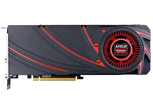
My, uh, lack of enthusiasm was dampened somewhat when the first example of the R9 285 arrived in Damage Labs. Behold the MSI Radeon R9 285 Gaming OC Edition.
This puppy is gorgeous, and its twin-fan cooler performs as well as its looks suggest. There’s good news on the performance front, too, since MSI has cranked up the Boost clock to 973MHz, 55MHz above stock.
At least MSI was doing good work with its part of the equation.
Theoretical Performance Concerns
Still, I thought, a snazzy cooler and paint job couldn’t fix the basic problem with the AMD Radeon R9 285. Although the new Radeon was up to snuff elsewhere, its memory bandwidth just looked a bit anemic.
Peak pixel
fill rate
(Gpixels/s)
Peak
bilinear
filtering
int8/fp16
(Gtexels/s)
Peak
shader
arithmetic
rate
(tflops)
Peak
rasterization
rate
(Gtris/s)
Memory
bandwidth
(GB/s)
Radeon
R9 280
30
104/52
3.3
1.9
240
Radeon
R9 285
29
103/51
3.3
3.7
176
Radeon
R9 280X
32
128/64
4.1
2.0
288
GeForce GTX
760
33
99/99
2.4
4.1
192
GeForce GTX 770
35
139/139
3.3
4.3
224
The MSI card’s higher boost clocks would give it a bit more oomph in some categories than the stock numbers shown for the R9 285 above, but it wouldn’t do anything to address the biggest issue.
The R9 285’s 176 GB/s of memory bandwidth is just a lot less than the R9 280’s 240 GB/s—and quite a bit less than what the competing GeForces have to offer, too.
Tonga’s Dilemma
So you can understand my reticence.
Tonga looked to be nothing more than a dreary re-spin of AMD’s existing technology, based on the same Radeon DNA as the Hawaii GPU introduced one year ago—and the Bonaire chip first outed in March of 2013. Those chips weren’t that different from the Tahiti GPU that debuted at the end of 2011.
To be fair, AMD did make some notable improvements in Hawaii and Bonaire.
Both of those chips have the TrueAudio DSP block onboard, so that games can offload audio processing to a dedicated hardware unit on the GPU. T
hose chips include a new XDMA data transfer mechanism for CrossFire, which allows frame data to be transferred via PCI Express instead of over an external bridge. Hawaii and Bonaire also have updated display outputs with support for the latest DisplayPort standards.
FreeSync and PowerTune Enhancements
In fact, AMD tells us that only Radeon cards based on Bonaire, Hawaii, and Tonga will support the variable refresh displays being enabled by its Project FreeSync initiative. I wasn’t aware that older Radeons would be excluded, but apparently they will.
One other addition in Hawaii—and now Tonga—is a smarter version of AMD’s PowerTune dynamic voltage and frequency scaling (DVFS) scheme.
The new PowerTune monitors the GPU’s current state constantly and makes fine-grained adjustments to clock speeds and supplied voltages in order to keep the GPU within its pre-defined thermal and power peaks.
The smarter PowerTune algorithm allows the graphics chip to squeeze out every ounce of performance possible within those limits.
Maxwell Is Underway
These tweaks are all well and good, and Hawaii in particular is a truly impressive GPU specimen, but they don’t do that much to improve the GPU’s fundamental performance or efficiency. Hawaii gets its potency from sheer scale more than anything else.
That reality was a problem for Tonga, in my view, because Maxwell is coming.
Nvidia has already released a small-scale version of its new GPU architecture aboard the GeForce GTX 750 Ti, and we know the little Maxwell is about twice as power-efficient as the corresponding chip based on the Kepler architecture.
Nvidia is widely rumored to be prepping larger Maxwell derivatives for release soon. Those chips are likely to convert this architecture’s increased power efficiency directly into higher performance. If Tonga were just a cost-reduced Tahiti chip with TrueAudio added, AMD could be in for a world of hurt.
Tonga: it’s a magical place
Turns out my worries were misplaced, because Tonga is not just a smaller version of Hawaii.
A year after the release of that bigger GPU, AMD has slipstreamed some significant new technology into Tonga—and has done so rather quietly, without a branding change or any of the usual fanfare.
In fact, I had to prod AMD a little bit in order to understand what’s new in Tonga. I don’t yet have a clear picture of how everything works, but I’ll share what I know.
Delta Color Compression: Game-Changing Technology
By far the most consequential innovation in Tonga is a new form of compression for frame buffer color data.
GPUs have long used various forms of compression in order to store color information more efficiently, but evidently, the method Tonga uses for frame buffer data is something novel. AMD says the compression is lossless, so it should have no impact on image quality, and “delta-based.”
Tonga’s graphics core knows how to read and write data in this compressed format, and the compression happens transparently, without any special support from applications.
We don’t have many details on exactly how it works, but essentially, “delta-based” means the compression method keys on change. My best bet is that whenever a newly completed frame is written to memory, only the pixels whose color have changed from the frame prior are updated.
ARM does something along those lines with its Mali mobile GPUs, and I expect AMD has taken a similar path.
Real-World Bandwidth Efficiency
The payoff is astounding: AMD claims 40% higher memory bandwidth efficiency. I’m not quite sure what the basis of comparison is for that claim, nor am I clear on whether 40% is the best-case scenario or just the general case. But whatever; we can measure these things.
3DMark Vantage’s color fill test has long been gated primarily by memory bandwidth, rather than the GPU’s raw pixel fill rate. Here’s how Tonga fares in it.
Compare the AMD Radeon R9 285 to the Radeon HD 7950 Boost, which we used in place of the Radeon R9 280. (Only 8MHz of clock speed separates them.) The 7950 Boost has 240 GB/s of memory bandwidth to Tonga’s 176 GB/s, yet the new Radeon maintains a substantially higher pixel fill rate. That’s Tonga magic in action.
Perhaps my concerns about Tonga’s memory bandwidth were premature. We’ll have to see how well this compression mojo works in real games, but it certainly has my attention.
Enhanced Geometry Processing
That’s not all. Tonga has inherited a new front-end and internal organization from Hawaii that grants it more potential for polygon throughput.
The triangle setup rate has doubled from two primitives per clock in Tahiti to four per clock in Tonga. Beyond that, Tonga adds some of its own provisions to improve geometry and tessellation performance, including a larger parameter cache that spills into the L2 cache when needed.
The division of work between the geometry front-end units has been improved, and these units can better re-use vertices, which AMD says should help performance in cases where “many small triangles” are present.
These architectural modifications more than bring the R9 285 up to par with its nearest rival, the GeForce GTX 760, in terms of geometry throughput. Tonga also surpasses the Hawaii-based Radeon R9 290X in this synthetic test of tessellation performance.
Media Processing: 4K
Between the new color compression method and the geometry performance gains, Tonga could plausibly claim to usher in a new generation of Radeon technology.
The use of the GCN or “Graphics Core Next” label has proven incredibly flexible inside the halls of AMD, but what we’re seeing here sure feels like a fundamental shift.
That’s not the full extent of the changes, either. AMD has revamped Tonga’s media processing capabilities in order to ensure fluid performance and high-quality images in the era of 4K video.
That starts with a new hardware image-scaling block in the display pipeline. This scaler is capable of upscaling to and downscaling from 4K video targets in real time.
In a related move, the graphics core has gained some new instructions for 16-bit integer and floating-point media and compute processing at reduced power levels.
Also, both the video decode (UVD) and encode (VCE) engines on Tonga have been upgraded to allow for higher throughput. The UVD block now supports the MJPEG standard and can decode high-frame-rate 4K video compliant with the High Profile Level 5.2 spec.
The beefier VCE block can encode 1080p video at 12X the real-time rate and is capable of encoding 4K video, as well.
We’ve had limited time to test Tonga, so we haven’t been able to scrutinize its video processing chops yet. Above are some encoding performance results that AMD supplied to reviewers showing the R9 285 outperforming the GeForce GTX 760. Make of them what you will.
But wait, there’s more!
The Full Tonga Silicon: What Lies Beneath
One of the strange things about Tonga’s introduction to the world is that it’s debuting in a product where’s its at less than full strength.
AMD hasn’t provided a ton of info about the full GPU, perhaps as a result of that fact, but below is my best guess at how Tonga looks from 10,000 feet.
The image above shows eight compute units per shader engine, with four shader engines across the chip.
AMD has confirmed to us that Tonga is indeed hiding four more compute units than are active in the R9 285, so the diagram above ought to be accurate in that regard. Here’s my best estimate of how Tonga stacks up in terms of key metrics versus its closest competition.
ROP
pixels/
clock
Texels
filtered/
clock
(int/fp16)
Shader
processors
Rasterized
triangles/
clock
Memory
interface
width (bits)
Estimated
transistor
count
(Millions)
Die
size
(mm²)
Fabrication
process node
GK104
32
128/128
1536
4
256
3500
294
28 nm
GK110
48
240/240
2880
5
384
7100
551
28 nm
Tahiti
32
128/64
2048
2
384
4310
365
28 nm
Tonga
32
128/64
2048
4
256
5000
359
28 nm
Hawaii
64
176/88
2816
4
512
6200
438
28 nm
Analyzing Die Size and Memory Interface
The die size and transistor count for Tonga above come directly from AMD. What fascinates me about these figures is that Tonga is barely any smaller than Tahiti. The idea that Tonga is a cost-reduced version of Tahiti pretty much goes out of the window right there.
Look at the transistor count, though. Tonga packs in roughly five billion transistors, while Tahiti is less complex, at 4.3 billion. Both chips are made at TMSC on a 28-nm process. How is it that Tonga’s not quite as large as Tahiti yet has more transistors?
Transistor Density Improvements
Since the chips are separated by three years, I suspect GCN compute units in Tonga are more densely packed than those in Tahiti. AMD has had more time to refine them.
That said, we know that the two GPUs have the same number of compute units, so presumably Tonga doesn’t get its much higher transistor count from its shader core.
All of the other additions we’ve talked about, including the TrueAudio DSP block, the color compression capability, and video block enhancements, add some complexity. I doubt they’re worth another 700 million transistors, though.
My best guess is that most of the additional transistors come from cache, perhaps a larger L2. SRAM arrays can be very dense, and a larger L2 cache would be a natural facilitator for Tonga’s apparently quite efficient use of memory bandwidth. I’ve pinged AMD about the size of Tonga’s L2 cache but haven’t heard back yet.
Hidden Memory Interface Potential
Another question these numbers raise is whether Tonga natively has a 256-bit memory interface.
Generally, the size of a chip like this one is dictated by the dimensions of the I/O ring around its perimeter. Since Tonga occupies almost the same area as Tahiti, it’s got to have room to accommodate a 384-bit GDDR5 interface.
Surely we’ll see a Radeon R9 285X card eventually with a fully-enabled Tonga GPU clocked at 1GHz or better. If I were betting, I’d put my money on that card having a 384-bit path to memory.
Game Testing the AMD Radeon R9 285
Testing Methodology
As ever, we did our best to deliver clean benchmark numbers. Our test systems were configured like so:
Processor
Core i7-3820
Motherboard
Gigabyte
X79-UD3
Chipset
Intel X79
Express
Memory size
16GB (4 DIMMs)
Memory type
Corsair
Vengeance CMZ16GX3M4X1600C9
DDR3 SDRAM at 1600MHz
Memory timings
9-9-9-24
1T
Chipset drivers
INF update
9.2.3.1023
Rapid Storage Technology Enterprise 3.6.0.1093
Audio
Integrated
X79/ALC898
with Realtek 6.0.1.7071 drivers
Hard drive
Kingston
HyperX 480GB SATA
Power supply
Corsair
AX850
OS
Windows
8.1 Pro
Driver
revision
GPU
base
core clock
(MHz)
GPU
boost
clock
(MHz)
Memory
clock
(MHz)
Memory
size
(GB)
Radeon
HD 7950 Boost
Catalyst 14.7 beta
2
–
925
1250
3072
Radeon
R9 285
Catalyst 14.7 beta
2
–
973
1375
2048
Radeon
R9 280X
Catalyst 14.7 beta
2
–
1000
1500
3072
GeForce
GTX 760
GeForce
340.52
980
1033
1502
2048
GeForce
GTX 770
GeForce
340.52
1046
1085
1753
2048
Thanks to Intel, Corsair, Kingston, and Gigabyte for helping to outfit our test rigs with some of the finest hardware available. AMD, Nvidia, and the makers of the various products supplied the graphics cards for testing, as well.
Also, our FCAT video capture and analysis rig has some pretty demanding storage requirements.
For it, Corsair has provided four 256GB Neutron SSDs, which we’ve assembled into a RAID 0 array for our primary capture storage device. When that array fills up, we copy the captured videos to our RAID 1 array, comprised of a pair of 4TB Black hard drives provided by WD.
Unless otherwise specified, image quality settings for the graphics cards were left at the control panel defaults. Vertical refresh sync (vsync) was disabled for all tests.
The tests and methods we employ are generally publicly available and reproducible. If you have questions about our methods, hit our forums to talk with us about them.
Watch Dogs
Yep, Tonga’s color compression magic translates pretty well into performance in real games.
The R9 285 effortlessly outperforms the AMD Radeon HD 7590 Boost—which, again, is essentially the same thing as the Radeon R9 280. (Sorry, didn’t realize until too late that Damage Labs didn’t have an R9 280 on hand, so you’ll have to settle for a different name on the graph labels.)
The newest Radeon also outdoes the GeForce GTX 760, its closest competitor, and that card’s bigger brother, the GTX 770.
These “time spent beyond X” graphs are meant to show “badness,” those instances where animation my be less than fluid—or at least less than perfect.
The 50-ms threshold is the most notable one, since it corresponds to a 20-FPS average.
We figure if you’re not rendering any faster than 20 FPS, even for a moment, then the user is likely to perceive a slowdown. 33 ms correlates to 30 FPS or a 30Hz refresh rate.
Go beyond that with vsync on, and you’re into the bad voodoo of quantization slowdowns. And 16.7 ms correlates to 60 FPS, that golden mark that we’d like to achieve (or surpass) for each and every frame.
Not only does the R9 285 perform well it terms of FPS averages, but it also generates new frames with consistent quickness. The new Radeon barely ever surpasses our 33-ms badness threshold.
In other words, the frame rate barely ever drops below 30 FPS, even for an instant. For that reason, Watch_Dogs is quite playable on the R9 285 at 2650×1440. In fact, that’s the display resolution AMD has identified as a good target for this card.
Crysis 3
Nvidia has done some nice work with its graphics drivers in the past year or so, cutting out cases where games slow down for whatever reason.
That work pays off here, as you can see in the plots, in the two places where I fire exploding arrows at the bad guys during our test run. The Radeons have a couple of big frame-time spikes in their plots, while the GeForces don’t.
Frame times are a little less variable overall on the GeForce cards, and that reflects in the 99th percentile results. Even though the R9 285 produces a slightly higher FPS average than the GeForce GTX 760, the GTX 760 comes out at ahead in our more time-sensitive metric.
The frame time curve reveals that the R9 285 generally outperform the GTX 760, but the GeForce is quicker in the most difficult two to three percent of frames.
My sense is that the frame time spikes and “badness” we see from the Radeons here is something AMD needs to fix with driver optimization. I doubt it’s a reflection on the underlying GPU tech. That said, it does reflect on the quality of the experience gamers will have with the product.
Borderlands 2
Since the last couple of games were a bit challenging for this class of GPU at 2560×1440, I thought I’d include my favorite game as an example of how well these cards can handle a fairly typical Unreal Engine 3-based title.
https://youtube.com/watch?v=hCTWFQfgC20%3Frel%3D0%26vq%3Dhd720
Wow. That Tonga devil magic does work wonders. The Radeon R9 285’s frame time plots illustrate how very consistently the GPU produces frames in this test scenario.
Although it doesn’t produce the most total frames (and thus doesn’t have the highest FPS average), the Radeon R9 285 takes the top spot in our 99th percentile frame time metric.
No matter which of our metrics you use, the AMD Radeon R9 285 handles Borderlands 2 flawlessly, ahead of both the GTX 760 and the 770. That latter card is based on a full-blown GK104 graphics processor. In our time-sensitive metrics, the R9 285 also beats the full-fledged Tahiti card, the Radeon R9 280X.
Thief
I decided to just use Thief‘s built-in automated benchmark, since we can’t measure performance with AMD’s Mantle API using Fraps. Unfortunately, this benchmark is pretty simplistic, with only FPS average and minimum numbers (as well as a maximum, for all that’s worth.)
Chalk up another shocking win for Tonga. The R9 285 beats both the R9 280X and the GeForce GTX 770 in the Thief benchmark. Good grief.
Notice that the R9 285 doesn’t fare as well with AMD’s close-to-the-metal Mantle API as it does with the game’s default Direct3D mode. By contrast, the Tahiti-based Radeon HD 7950 benefits a bit from the switch to Mantle. Looks to me like Mantle support for the R9 285 may not quite be ready for prime time.
Power Consumption
Please note that our “under load” tests aren’t conducted in an absolute peak scenario. Instead, we have the cards running a real game, Crysis 3, in order to show us power draw with a more typical workload.
AMD hinted that the R9 285 ought to be more power-efficient than its older Tahiti-based graphics cards.
In our tests, under load, that’s not the case. I suspect the cause of the disconnect here may be the fact that MSI has pushed the frequency up—and likely the voltage, as well—on this Radeon R9 285 Gaming OC Edition card.
Given the performance that we’ve seen out of this card, though, its power efficiency seems pretty reasonable.
Noise Levels and GPU Temperatures
This dual-fan MSI cooler is scary good. As I tested, I thought subjectively that the R9 285 card got quieter under load than it was at idle. Then, uh, the meter confirmed it.
MSI has been very aggressive in choosing a 65°C tuning point for its R9 285 card. With the new PowerTune, AMD has typically exploited quite bit more temperature headroom. In truth, though, the R9 285 doesn’t seem to need it.
Closing Thoughts of the AMD Radeon R9 295
I haven’t yet had time to test the AMD Radeon R9 285 as extensively as I’d like. I had to throw together this review in a few days after finishing up the Core i7-5960X, and there just wasn’t time to test more games or display resolutions.
That said, I think we have a sense of how surprisingly potent this video card really is, thanks to a GPU that’s packed with more innovation than we expected.
Here’s one more reminder of how wildly this card is overachieving given its memory bandwidth. We’re averaging together the results from all of our game tests here.
Compared to the Radeon HD 7950, the R9 285 is a big move up and to the left, in the direction of goodness. The R9 285 easily makes the most effective use of its memory bandwidth of any of the cards we tested. Like I said earlier, this is generational change on the GPU front.
AMD Radeon R9 285: Is the Price Tag Justified?
Our famous value scatter plot tells the rest of the story. In our limited tests, the R9 285 looks to be fast enough to justify its $249 price tag pretty well. I suppose that’s what AMD was thinking, huh? The GeForce GTX 770 sure looks like a raw deal by comparison.
This MSI Gaming OC Edition card is a stone cold killer, too. I’m smitten. MSI has nailed it with this cooler and the board’s overall design.
Bundle Value and Availability
Consider also that AMD is throwing in a trio of games via its Never Settle bundle with the purchase of an AMD Radeon R9 285, and you might be tempted to order one right away.
I can’t say I’d blame you. R9 285 cards are supposed to be on store shelves today, and AMD tells us it expects an ample initial supply. Most of them will have 2GB of memory, but there will be 4GB variants coming, as well.
Only thing is, I’m pretty sure this is the opening salvo of a protracted battle. If I’m right about Tonga having a 384-bit interface, then the AMD Radeon R9 285X could turn out to be quite the thrill ride.
We don’t yet know exactly what Nvidia has cooking, either, but it may well be a Maxwell variant that’s direct competition for Tonga. I suspect we’ll have more reasons to test this magical new GPU in the coming weeks.
The Tech Report editorial policy is centered on providing helpful, accurate content that offers real value to our readers. We only work with experienced writers who have specific knowledge in the topics they cover, including latest developments in technology, online privacy, cryptocurrencies, software, and more. Our editorial policy ensures that each topic is researched and curated by our in-house editors. We maintain rigorous journalistic standards, and every article is 100% written by real authors.
